Laser Seismograph
My manager at work approached me one day and asked if there was a PCB I’d like to make, to help the company create a rapid prototyping process. I jumped at the opportunity and decided to build a seismograph for my apartment which uses a swinging laser pendulum to detect low frequency movement of the building.
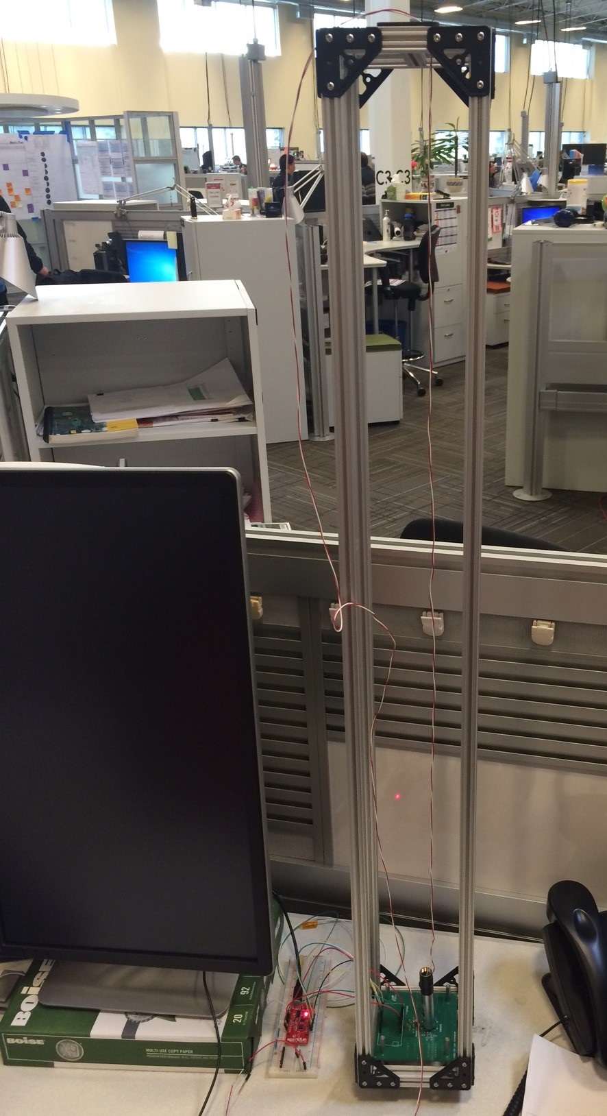
The almost completed final product- a 1m long pendulum with a laser at the end, hanging above four photodiodes. The red microcontroller board is supposed to fit onto the PCB directly but I need to do some cut-and-jumper mods first.
The central idea for the project came from an article by Forrest Mims in Make Magazine, which used a laser pendulum and a single photodiode to look for movement. I extended that idea to four photodiodes to see direction of movement, and I used the ESP8266 microcontroller to enable wireless transmission of data so I wouldn’t need a long cord between rooms of my apartment.
The theory of operation is that a long enough pendulum will have observable movement if the thing it is mounted to sways back and forth. So, in my concrete apartment tower, if I were to hang a pendulum from the ceiling I might be able to notice if the building was swaying due to wind, nearby construction, earthquakes, or other external forces. Instead of creating such a large apparatus I stuck with a 1m pendulum, a decision led mostly by the availability of OpenBeam aluminum struts that are 1m long. For the laser I just took apart a cheap laser pointer that I got years ago at a career fair.
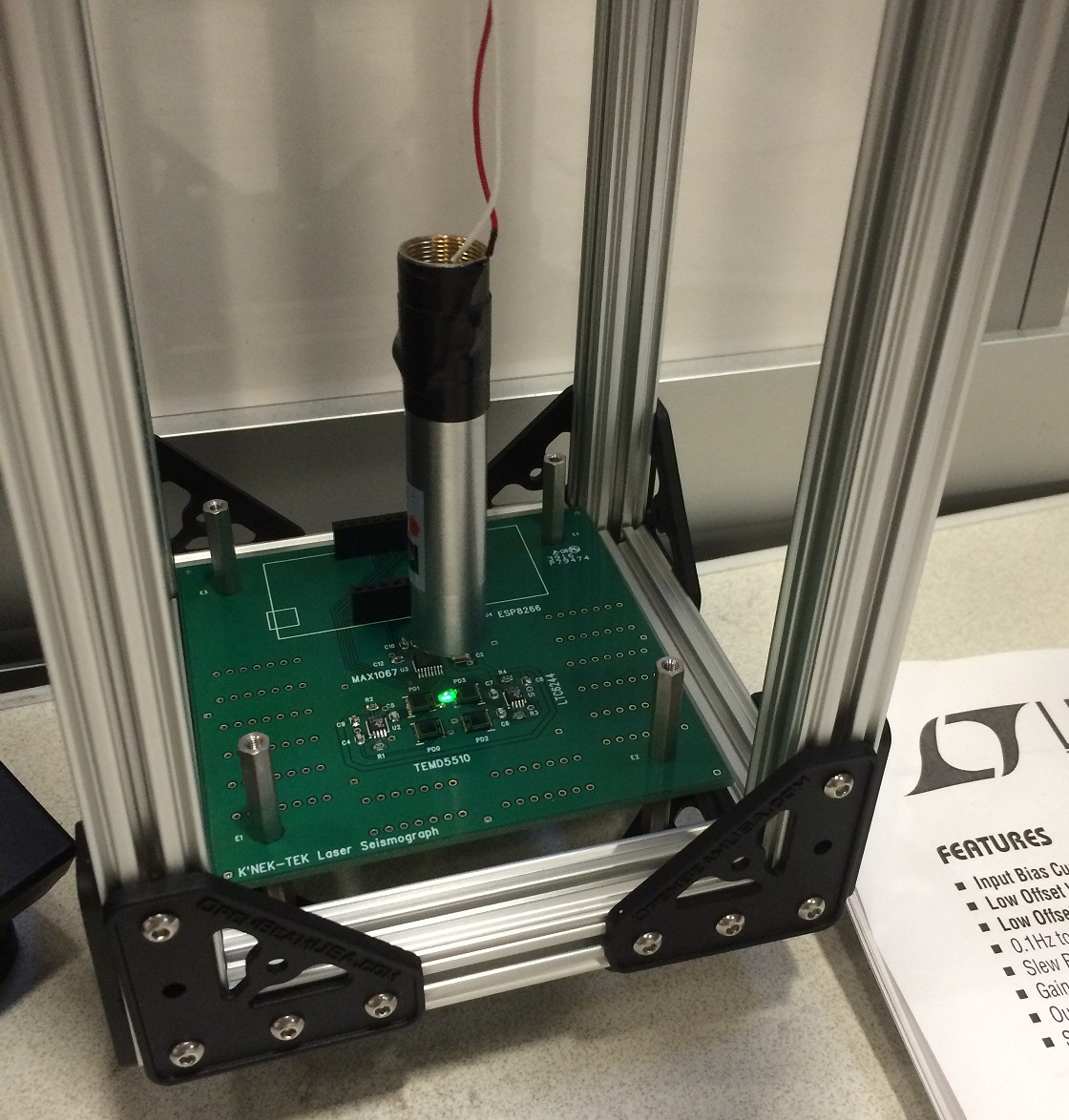
Closeup on the pendulum as it hangs above the four photodiodes.
As an electrical engineer the main aspect of this project that worried me was the large mechanical element, specifically building a frame, mounting the pendulum inside in a way that wouldn’t bias the motion, and mounting the whole apparatus in a corner of my apartment. The device needs to be closely coupled into the building to be able to observe minute movements. After talking with a friend who is a mechanical engineer I concluded that attaching it to two walls in a corner with four fasteners should do the trick. He also introduced me to OpenBeam which makes building a frame much easier, since I had never worked with extruded aluminum or any kind of metallic scaffolding before.
The system uses 3.3V and 5V, both provided by the ESP8266 Thing Dev board through a USB power connection. I chose 5V for the photodiode amplification circuit to get the maximum range of detection, and the MAX1067 (link goes to PDF) 14-bit ADC which is able to use 5V and 3.3V at the same time, letting me not only convert from analog to digital but transition between voltage levels since the ESP8266 is strictly 3.3V. The photodiodes, which have their most sensitive range at the same 530nm the laser uses, convert light into current and that signal gets amplified by the LT6244 opamps. From there it goes to the ADC, and the data comes over SPI to the microcontroller up to 100 readings per second. I chose to do 5 readings per second because the microcontroller is very busy transmitting the data wirelessly to my router and that is a huge bottleneck. If I try to send the four integers representing the four photodiodes at 100Hz, or even 10Hz, much of the data gets dropped or arrives out of order. Also for a very low-frequency seismograph like this, observing swings of the pendulum at 5-10Hz is enough to get directionality and magnitude.
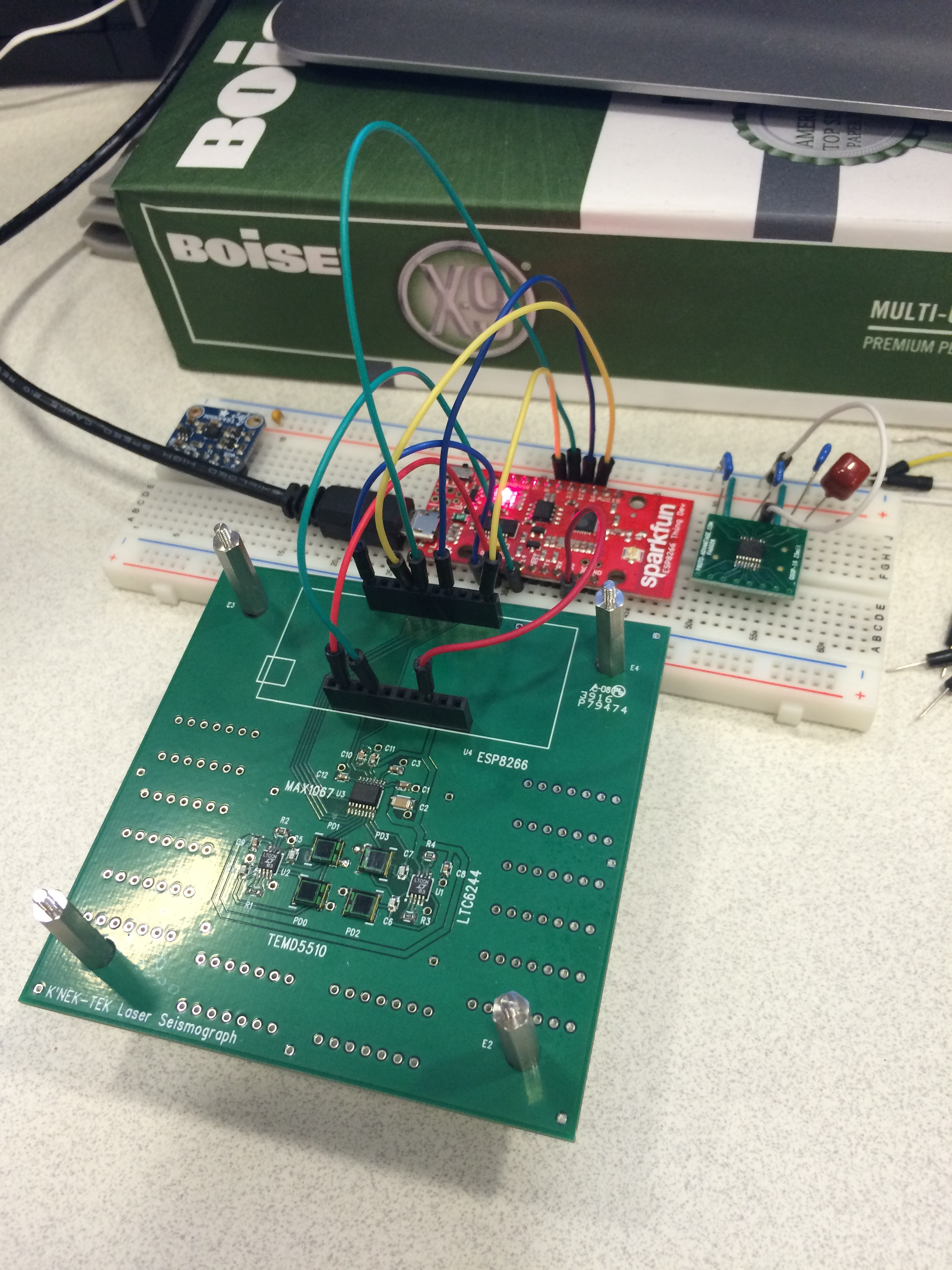
Closeup of the PCB with the microcontroller jumpered in to the sockets where it will fit. Due to the poor datasheet that sparkfun provided for the ESP8266 Thing Dev, the pin usage I had planned didn’t work and I had to use different pins for different functions, so those black sockets won’t work until I cut some traces and jumper some wires around. Then I’ll be able to plug in the Thing Dev board directly to the PCB. In this photo the MMA8451 is the blue chip at left, and the another MAX1067 ADC on a breakout board to the right that I used for directly debugging the software interface for the uC <-> ADC.
To learn how to wire up the photodiodes to amplify their signal, I relied on several papers such as this one by TI (opens a PDF). There are several different topologies that can be used with a photodiode and opamp and I just chose the simplest one with the fewest components. Extensive simulations of various Rf and Cf values along with a current source that approximated the chosen photodiodes (as closely as I could manage) let me select Rf and Cf values that ended up working out wonderfully. I did not have to tune the opamp circuit once I built it- the signal from the laser comes through cleanly without clipping against the power rails, while ambient light in a brightly lit office is low enough that I didn’t need to add walls to the tower as originally planned.
Closeup of the PCB in frame. The photodiodes are the TEMD5510.

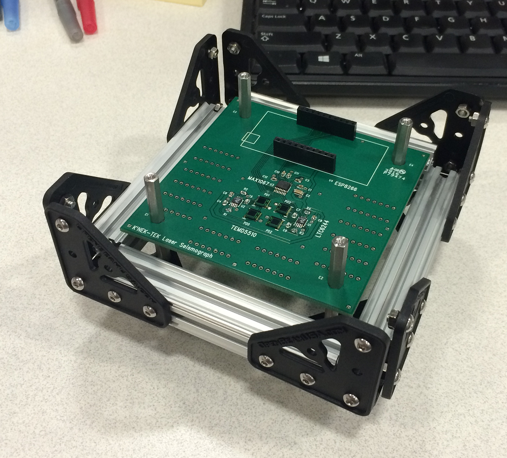
Closeup of the underside of the PCB in frame.
Initially I wanted to collect and graph the data using Sparkfun’s Phant service at data.sparkfun.com, but unfortunately they have a rate limit of 100 posts per 15 minutes. Phant’s built-in data visualization service would not be able to pull apart a compressed data item, for example if I sent the four values as one piece of data to get 4x the throughput. So, I will have to collect and graph the data on a server in my apartment. In the past I’ve had good luck with Dygraphs, or Gnu Octave. To produce an image of early results I just used a Processing script to grab the data and write to a .csv file, then Excel to clean it up and graph it:
The signal from the four photodiodes over time after pushing the pendulum twice. Sorry that it’s such a wide image! :-/
Calendar time on this project was four months, September-December 2016, which is dang fast for a hobby project. The reason I was able to get so much done is because my boss let me spend down-time at work on it, letting me fill in gaps between my “real” work. That helps quite a bit for forcing me to focus, since I get easily distracted from projects I do at home.
A stretch goal for this project was to add the MMA8451 accelerometer breakout board from Adafruit, to provide several features: first, a high precision accelerometer is a good seismograph on its own! Second, the accelerometer would let me do a calibration on startup of how level the PCB is in the frame. If the Z axis doesn’t show -9.8m/s^2, and the X- and Y-axes are non-zero, then I could use geometry and the device’s calibration registers to figure out how much the board is tilted and in what direction, then calibrate for that. Third, I could add jostle detection to determine if the apparatus was bumped and therefore the data should be ignored for the next minute or two.
I made a list of lessons learned from this project which others might find useful:
1) Use the largest, easiest to rework parts as possible. Instead of 0603 components, I really could have gotten away with 1206 or 1210 pads for the passives especially around the opamps. Thankfully I didn’t have to swap out R and C in the opamp circuitry to tune the amplifier (yay simulations!) but if I had this would have been a soldering challenge.
2) On a board with this much extra space, place multiple footprint sizes on the same net so I can use the components I find even if they’re not the exact right footprint. For example, an 0805 footprint in parallel with an 0603 and 1206 footprint would let me choose any of those sizes if I needed to swap out resistors or capacitors.
3) This board had several rows of holes in case I wanted to solder in more components (like the MMA8451 mentioned above). Those rows should be a variety of sizes to fit 8-pin, 12-pin, 14-pin DIPs.
4) * This is a big one: I should have waited to make the PCB until after I had soldered the ADC to a DIP breakout board and gotten all the software working on a breadboard, with just the ESP8266 and the ADC. This eliminates lots of other variables and then when it is 100% ready I can move to layout. That way I could avoid finding out too late that the spare digital IO pins on the ESP8266 Thing Dev board are actually used for a variety of other things not mentioned in Sparkfun’s graphical datasheet. That datasheet hides a lot of important info and caused me some setbacks.
5) Net names should be on the PCB silkscreen next to the pins for the uC sockets. That way when I am plugging in jumper wires to hook the ESP8266 into the board, I know which pins are what without having to constantly reference the layout files.
6) I should have added through-hole test points on many of the digital and analog nets so I could attach test hoops, for hooking up oscilloscope probes to different traces. I wasn’t able to debug the SPI channel on the board because I would have had to solder very fine wires to the ADC and attached oscilloscope probes to those.
7) Those through-hole test points mentioned above would have also made cut-and-jumper mods much easier. As it is, I need to cut several traces and add jumpers directly to the ADC’s tiny little pins, rather than having a nice through-hole to solder to on those nets.
Tl;dr: Don’t trust datasheets, verify usage of every component with the microcontroller on a breadboard one by one before doing layout. :-)
UPDATE: I have uploaded the schematic, layout files, and software to github: https://github.com/Erik-k/LaserSeismograph